- 您现在的位置:买卖IC网 > Sheet目录1997 > ICS841602AGILF (IDT, Integrated Device Technology Inc)IC CLOCK GENERATOR 28-TSSOP
FEMTOCLOCKS CRYSTAL-TO-HCSL
CLOCK GENERATOR
ICS841602I
IDT / ICS HCSL CLOCK GENERATOR
1
ICS841602AGI REV. A JULY 10, 2008
GENERAL DESCRIPTION
The ICS841602I is an optimized PCIe and
sRIO clock generator and member of the
HiPerClocks family of high-performance clock
solutions from IDT. The device uses a 25MHz
parallel crystal to generate 100MHz and 125MHz
clock signals, replacing solutions requiring multiple oscilla-
tor and fanout buffer solutions. The device has excellent
phase jitter (< 1ps rms) suitable to clock components requiring
precise and low-jitter PCIe or sRIO or both clock signals.
Designed for telecom, networ king and industr ial appli-
cations, the ICS841602I can also drive the high-speed sRIO
and PCIe SerDes clock inputs of communication processors,
DSPs, switches and bridges.
FEATURES
Two differential clock outputs: configurable for PCIe (100MHz)
and sRIO (125MHz) clock signals
Selectable crystal oscillator interface, 25MHz, 18pF parallel
resonant crystal or LVCMOS/LVTTL single-ended reference
clock input
Supports the following output frequencies:
100MHz or 125MHz
VCO: 500MHz
PLL bypass and output enable
PCI Express (2.5Gb/s) and Gen 2 (5 Gb/s) jitter compliant
RMS phase jitter, 125MHz, using a 25MHz crystal:
(1.875MHz – 20MHz): 0.45ps (typical)
Full 3.3V power supply mode
-40°C to 85°C ambient operating temperature
Available in both standard (RoHS 5) and lead-free (RoHS 6)
packages
HiPerClockS
ICS
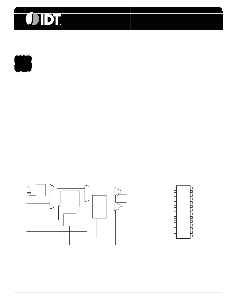
BLOCK DIAGRAM
0
1
0
M = ÷20
OSC
FemtoClock
PLL
VCO = 500MHz
÷N
÷4
÷5 (default)
XTAL_IN
XTAL_OUT
REF_SEL
FSEL
MR/nOE
IREF
BYPASS
REF_IN Pulldown
Pulldown
Q0
nQ0
Q1
nQ1
PIN ASSIGNMENT
1
2
3
4
5
6
7
8
9
10
11
12
13
14
28
27
26
25
24
23
22
21
20
19
18
17
16
15
ICS841602I
28-Lead TSSOP
6.1mm x 9.7mm x 0.925mm
package body
G Package
Top View
REF_SEL
REF_IN
VDD
GND
XTAL_IN
XTAL_OUT
MR/nOE
VDD
nc
GND
VDD
VDDA
BYPASS
IREF
FSEL
VDD
nQ1
Q1
nQ0
Q0
GND
nc
发布紧急采购,3分钟左右您将得到回复。
相关PDF资料
ICS841608AKI
IC CLOCK GENERATOR 32-VFQFPN
ICS841S012DKILF
IC FREQ SYNTHESIZER 56VFQFN
ICS842023BGLF
IC CLK GEN ETHERNET 25MHZ 8TSSOP
ICS8421002AGILF
IC FREQ SYNTHESIZER 20-TSSOP
ICS8422002AGILF
IC SYNTHESIZER LVHSTL 20-TSSOP
ICS8427DY-02LF
IC SYNTHESIZER 500MHZ 32-LQFP
ICS843001AG-123LF
IC SYNTHESIZER LVPECL 8-TSSOP
ICS843001AG-21LFT
IC SYNTHESIZER LVPECL 24-TSSOP
相关代理商/技术参数
ICS841602AGILFT
功能描述:IC CLOCK GENERATOR 28-TSSOP RoHS:是 类别:集成电路 (IC) >> 时钟/计时 - 时钟发生器,PLL,频率合成器 系列:HiPerClockS™, FemtoClock™ 标准包装:1,000 系列:- 类型:时钟/频率合成器,扇出分配 PLL:- 输入:- 输出:- 电路数:- 比率 - 输入:输出:- 差分 - 输入:输出:- 频率 - 最大:- 除法器/乘法器:- 电源电压:- 工作温度:- 安装类型:表面贴装 封装/外壳:56-VFQFN 裸露焊盘 供应商设备封装:56-VFQFP-EP(8x8) 包装:带卷 (TR) 其它名称:844S012AKI-01LFT
ICS841604AGILF
功能描述:IC CLOCK GENERATOR 28-TSSOP RoHS:是 类别:集成电路 (IC) >> 时钟/计时 - 时钟发生器,PLL,频率合成器 系列:HiPerClockS™, FemtoClock™ 标准包装:2,000 系列:- 类型:PLL 频率合成器 PLL:是 输入:晶体 输出:时钟 电路数:1 比率 - 输入:输出:1:1 差分 - 输入:输出:无/无 频率 - 最大:1GHz 除法器/乘法器:是/无 电源电压:4.5 V ~ 5.5 V 工作温度:-20°C ~ 85°C 安装类型:表面贴装 封装/外壳:16-LSSOP(0.175",4.40mm 宽) 供应商设备封装:16-SSOP 包装:带卷 (TR) 其它名称:NJW1504V-TE1-NDNJW1504V-TE1TR
ICS841604AGILFT
功能描述:IC CLOCK GENERATOR 28-TSSOP RoHS:是 类别:集成电路 (IC) >> 时钟/计时 - 时钟发生器,PLL,频率合成器 系列:HiPerClockS™, FemtoClock™ 标准包装:1,000 系列:- 类型:时钟/频率合成器,扇出分配 PLL:- 输入:- 输出:- 电路数:- 比率 - 输入:输出:- 差分 - 输入:输出:- 频率 - 最大:- 除法器/乘法器:- 电源电压:- 工作温度:- 安装类型:表面贴装 封装/外壳:56-VFQFN 裸露焊盘 供应商设备封装:56-VFQFP-EP(8x8) 包装:带卷 (TR) 其它名称:844S012AKI-01LFT
ICS841608AKI
功能描述:IC CLOCK GENERATOR 32-VFQFPN RoHS:否 类别:集成电路 (IC) >> 时钟/计时 - 时钟发生器,PLL,频率合成器 系列:HiPerClockS™, FemtoClock™ 标准包装:1,000 系列:- 类型:时钟/频率合成器,扇出分配 PLL:- 输入:- 输出:- 电路数:- 比率 - 输入:输出:- 差分 - 输入:输出:- 频率 - 最大:- 除法器/乘法器:- 电源电压:- 工作温度:- 安装类型:表面贴装 封装/外壳:56-VFQFN 裸露焊盘 供应商设备封装:56-VFQFP-EP(8x8) 包装:带卷 (TR) 其它名称:844S012AKI-01LFT
ICS841608AKILF
功能描述:IC CLOCK GENERATOR 32VFQFPN RoHS:是 类别:集成电路 (IC) >> 时钟/计时 - 时钟发生器,PLL,频率合成器 系列:HiPerClockS™, FemtoClock™ 标准包装:2,000 系列:- 类型:PLL 频率合成器 PLL:是 输入:晶体 输出:时钟 电路数:1 比率 - 输入:输出:1:1 差分 - 输入:输出:无/无 频率 - 最大:1GHz 除法器/乘法器:是/无 电源电压:4.5 V ~ 5.5 V 工作温度:-20°C ~ 85°C 安装类型:表面贴装 封装/外壳:16-LSSOP(0.175",4.40mm 宽) 供应商设备封装:16-SSOP 包装:带卷 (TR) 其它名称:NJW1504V-TE1-NDNJW1504V-TE1TR
ICS841608AKILFT
功能描述:IC CLOCK GENERATOR 32-VFQFPN RoHS:是 类别:集成电路 (IC) >> 时钟/计时 - 时钟发生器,PLL,频率合成器 系列:HiPerClockS™, FemtoClock™ 标准包装:1,000 系列:- 类型:时钟/频率合成器,扇出分配 PLL:- 输入:- 输出:- 电路数:- 比率 - 输入:输出:- 差分 - 输入:输出:- 频率 - 最大:- 除法器/乘法器:- 电源电压:- 工作温度:- 安装类型:表面贴装 封装/外壳:56-VFQFN 裸露焊盘 供应商设备封装:56-VFQFP-EP(8x8) 包装:带卷 (TR) 其它名称:844S012AKI-01LFT
ICS841608AKIT
功能描述:IC CLOCK GENERATOR 32-VFQFPN RoHS:否 类别:集成电路 (IC) >> 时钟/计时 - 时钟发生器,PLL,频率合成器 系列:HiPerClockS™, FemtoClock™ 标准包装:1,000 系列:- 类型:时钟/频率合成器,扇出分配 PLL:- 输入:- 输出:- 电路数:- 比率 - 输入:输出:- 差分 - 输入:输出:- 频率 - 最大:- 除法器/乘法器:- 电源电压:- 工作温度:- 安装类型:表面贴装 封装/外壳:56-VFQFN 裸露焊盘 供应商设备封装:56-VFQFP-EP(8x8) 包装:带卷 (TR) 其它名称:844S012AKI-01LFT
ICS841608I
制造商:IDT 制造商全称:Integrated Device Technology 功能描述:FEMTOCLOCKS CRYSTAL-TO-HCSL CLOCK GENERATOR VCO: 500MHz